Semiconductor
Testing the Advanced Products of Top Manufacturers.
The world’s number one contact solutions company.
For contact technology indispensable for semiconductor pre-shipment inspection,
Enplas has earned a top level reputation from the world’s leading semiconductor manufacturers.
Excellent development capabilities, proprietary applied technology of high-performance resin,
and an unwavering quality assurance system contribute to the development and mass production of semiconductors.
Full lineup of general-purpose IC sockets.
With ultra-multi pin count and fine pitch, our general-purpose IC socket lineup corresponds to every need.
For semiconductor burn-in sockets for thermal acceleration tests, and test sockets for semiconductor electrical testing, we continue to hold a high market share all over the world.
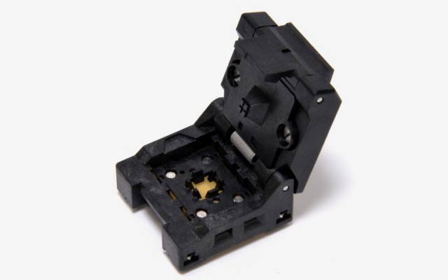 Ultra-fine pitch WCSP burn-in socket (0.3 mm pitch)
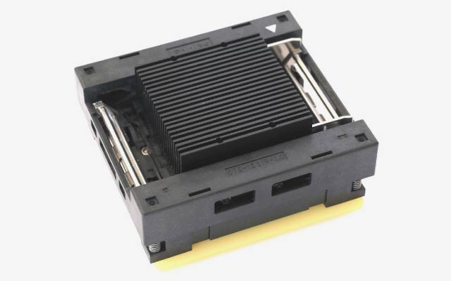 Multi-pin BGA burn-in socket with heat sink
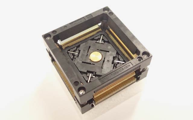 QFP burn-in socket with ground pin
Our development teams around the world conduct farsighted technology development while keeping a close watch on trends in semiconductors.
Coating technology for enhanced durability, solutions that enable measurement of higher frequencies, and thermal resistance technology that enables rating at higher temperatures-these are some of the IC socket contact solutions available from Enplas.
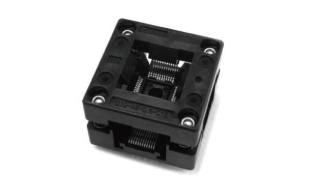
Silver plating technology
The ES plating (high temperature burn-in solution) prevents oxidation and extends the life of contact pins by forming an alloy with the solder during cycling.
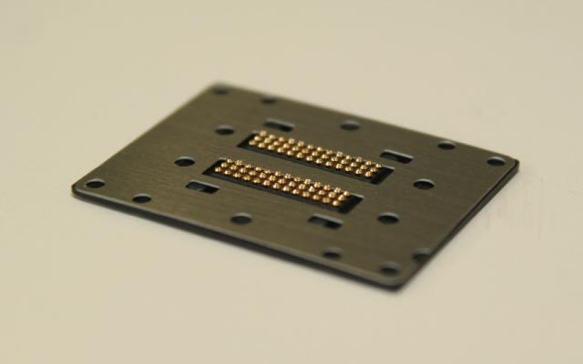
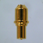
High-frequency solutions
By shortening the overall length, inductance is reduced to achieve stable high-frequency measurement “capsule contact”.
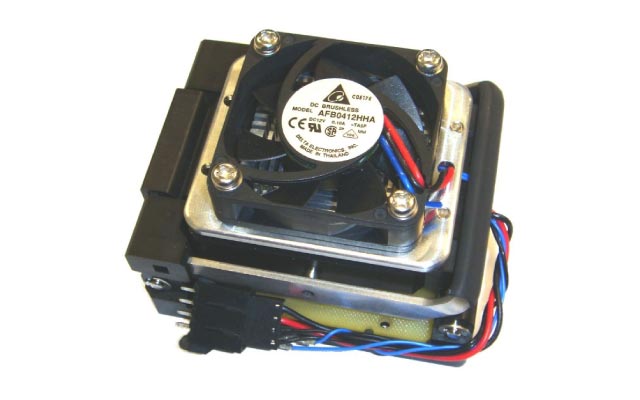
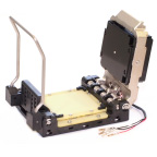
High power socket
An ancillary heat sink and sensor in the socket allows for simulation and achieves a shortened development delivery time.
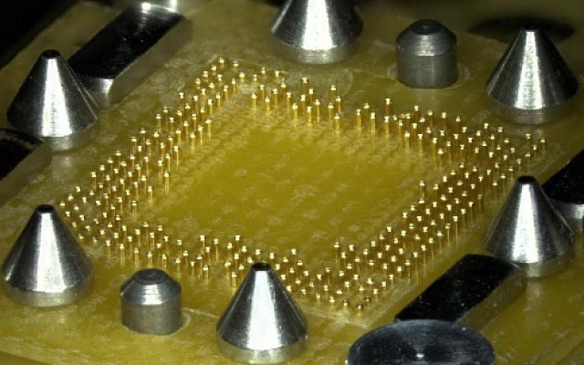
Ultra-fine 0.25mm pitch socket
Corresponding to high quality ultra-fine and multi-pin.
0.25mm pitch, realizing more than 3,000 pins.
Quickly addressing the need of highly-integrated super-multi pin semiconductors, and fine pitch. Through the application of our proprietary microfabrication and advanced resin technology, we provide burn-in sockets for IC tests with 0.25mm pitch and more than 3,000 pins. Contributing to the development and production of continuously evolving semiconductors.
Simulation technology
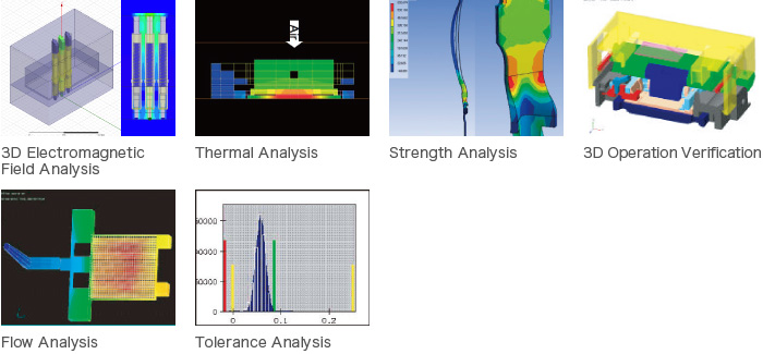
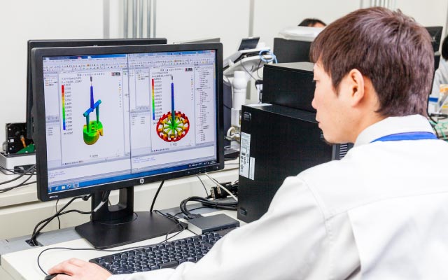
For contact technology solutions, we developed new simulation technologies that make full use of three-dimensional CAD, helping customers’ engineering design.
— Thermal analysis —
Verifying the heat dissipation through the heat sink in order to optimize socket materials and shape.
— Strength analysis —
Strength analysis conducted on molded parts and contact pins is reflected in IC socket design.
— 3D operation verification —
A three-dimensional perspective of the finished IC socket product, to verify the performance of the structure.
Basic technology
Corresponding to a wide variety of products, small lot production, and short delivery times.
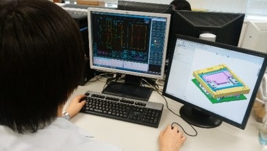
Design and development making full use of advanced 3D technology.
Design capabilities that make full use of three-dimensional CAD simulation technology. Things such as 3D automatic measurement technology allows us to meet more sophisticated requirements and construct a very high-level environment for design and development. Exercising full command of a variety of tools for multifaceted analysis, we have established a system that can deliver reliable products in a timely manner.
An original production system that enables short delivery times.
Automated assembly production system. A flexible production system that can respond to a wide variety of products. This unique system can reliably produce a mix of small lots all with short lead times.
Main Simulation Technology
